
TOPCO Well Poised to Mark Presence in Third-Generation Semiconductor Market, Seizing Opportunities in Advanced Packaging and High-Performance Substrates
2023 SEMICON Taiwan is set to take place from September 6th to 8th at Taipei Nangang Exhibition Center. Topco Scientific (TOPCO), a leading integrated service provider of critical semiconductor and optoelectronic materials, will showcase its comprehensive semiconductor supply chain solutions on the 4th floor of Hall 1. TOPCO will exhibit semiconductor integration services, front-end semiconductor manufacturing processes, advanced back-end packaging and high-performance substrates, pre-owned equipment and spare parts services, as well as comprehensive solutions for plant construction and factory management systems.
To share the latest innovative technologies and products, TOPCO is set to present “Composite Substrates Enabling True GaN World” and “3D IC Chip Stacking Metal Wire Bonding Interconnection Technology,” on the TechXPOT stage on September 7th. These advancements provide high-quality, large-sized, and low warpage GaN on QST wafers for third-generation semiconductors, as well as metal wiring solutions for advanced semiconductor packaging processes.
TOPCO Well Poised to Mark Presence in Third-Generation Semiconductor Market, Seizing Opportunities in Advanced Packaging and High-Performance Substrates
With an exponential rise in demand driven by 5G communication, consumer electronics, industrial energy conversion, and electric vehicles, TOPCO is highly optimistic about the third-generation semiconductor market for high-frequency communication and high-power applications. Collaborating with Japan’s Shin-Etsu Chemical, TOPCO is actively developing applications for gallium nitride (GaN) chip processes.
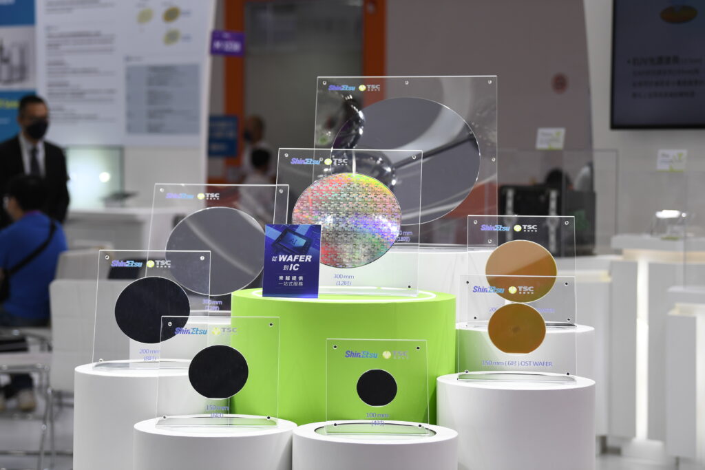
TOPCO is excited to invite Mr. Masato Yamada, Director of Shin-Etsu Chemical, to deliver a presentation titled “Composite Substrates Enabling True GaN World” and introduce the GaN on QST (Qromis Substrate Technology) technology, which features high quality, large size and low warpage characteristics.
Compared to conventional sapphire substrates and silicon-based (Si) substrates, QST substrates offer superior heat dissipation performance. Furthermore, the rapid switching frequency, high breakdown voltage, high thermal conductivity, and low drain-source on-state resistance characteristics of GaN drive the development of higher-performance transistors and integrated circuits. Compared to traditional silicon substrates, QST substrates exhibit a thermal expansion coefficient closer to that of GaN. During the epitaxial growth of GaN, using QST substrates significantly enhances the epitaxial yield, reducing chip warpage and wafer breakage. This improvement in yield can effectively expedite the manufacturing process and facilitate mass production in semiconductor foundries.
As the official agent and distributor for Shin-Etsu Chemical’s 6-inch and 8-inch GaN on QST wafers, TOPCO has established collaborations with domestic foundries to meet customer product demands. Furthermore, TOPCO has also developed production technology for 12-inch QST wafers, meeting the anticipated manufacturing requirements for large-sized GaN products from customers. Due to the strong demand driven by consumer electronics, 5G communication, and automotive electronics, the future prospects for GaN applications are expected to grow rapidly, which is anticipated to contribute to the accelerated growth momentum of TOPCO.
Capturing a Share of the Advanced Packaging Market with Chip-On-Wafer-On-Substrate (CoWoS) Technology: TOPCO Introduces 3D IC Chip Stacking with Metal Wire Bonding Interconnection Technology
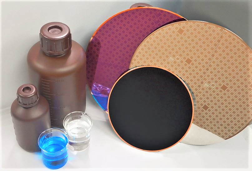
With the robust demand for AI applications, there’s a surge in demand for advanced process materials like 5nm and 3nm nodes, as well as for advanced packaging capabilities like CoWoS and 3D IC. TOPCO has announced the “Plating Chemical Products for Advanced Packaging Process” in response to the development of advanced semiconductor packaging processes.
In the pursuit of maximizing performance, increasing the number of interconnections is inevitable. However, metal bonding technology has encountered various new challenges, including minimizing the spacing and size between contact points to the maximum extent, as well as addressing thermal stress issues arising from larger substrate sizes. In collaboration with Mitsubishi Chemical, TOPCO is addressing these two major market trends by offering three new types of electroplating materials as solutions. These include “Nano-Porous Copper Structure Bonding Technology,” “Low-Temperature Soldering Indium Plating Technology” and “Substrate Plating Technology.”
To address issues arising from varying heights in the plating of copper pillars in the packaging process leading to poor bonding and voids, the “Nano-Porous Copper Structure Bonding Technology” eliminates the need for preliminary steps such as Chemical Mechanical Polishing (CMP) or plasma activation during the bonding process. This not only improves yield and streamlines the process, reducing costs, but also provides better electrical resistance and bonding performance compared to copper pillars paired with solder.
With the increasing size of substrates, the existing soldering processes tend to cause warping issues when subjected to high temperatures. To address this issue, TOPCO has introduced the “Low-Temperature Soldering Indium Plating Technology,” which utilizes indium as the electroplating material. This technique not only enables low-temperature soldering but also exhibits excellent formability and a lack of voids. It offers impressive reliability and achieves a high level of control over alpha particles, reaching SULA levels to avoid soft errors.
Furthermore, to overcome defects caused by the use of solder balls on closely spaced substrates, “Substrate Plating Technology” is employed as a substitute for solder paste. This technology achieves defect-free one-time plating of protruding points, showcasing impressive height uniformity. This unique additive technology can be applied for plating on substrates of different diameters, ensuring excellent coplanarity and a void-free effect, ultimately enhancing production efficiency.
Topco Scientific Joins 2023 SEMICON Taiwan at Nangang Exhibition Center, September 6th -8th
▍Booth information at 2023 SEMICON Taipei
◆Time: 10:00 – 17:00, September 6th -8th, 2023
◆Location: Booth#M1138 & M1148, 4F, Hall 1, Taipei Nangang Exhibition Center (No. 1, Jingmao 2nd Rd., Nangang Dist., Taipei)
▍TechXPOT
◆Time: PM 13:40-14:00 / 15:00-15:20, September 7th, 2023
◆Location:Booth#L1100, 4F, Hall 1, Taipei Nangang Exhibition Center
◆Topic:
13:40-14:00 Composite Substrates Enabling true GaN world : QST
15:00-15:20 Plating Chemical Products for Advanced Packaging Process
▍Technical Support Contact
Mr. Arthur Chen +886-3-564-2132#3448 arthur.chen@topco-global.com
Mr. Gary Yi +886-2-8797-8020#2859 gary.yi@topco-global.com
Share
Press Contacts
Della Huang
- TOPCO SCIENTIFIC CO.,LTD.
- Senior Deputy General Manager
- Stock Affair Office
Luyi Wu
- TOPCO SCIENTIFIC CO.,LTD.
- Manager
- Marketing & PR Dept.