Standard Sample Sales
Molded Sample Sales
We sell molding samples for the purpose of providing customers with an initial study of nanoimprinting technology.
Production Intro
Molded Sample Sales
We sell molding samples for the purpose of providing customers with an initial study of nanoimprinting technology.
Please inquire for the details.
■Pattern Size: Submicron~a few μm
■Substrate Size: φ2″, φ4″, φ6″
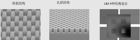
Resin Film
Glass Substrate
We can provide a processed sample onto glass substrate.
List of Nanoimprint Molding Examples
- Material: Optical Film (Thickness: 100μm~188μm)
- Other conditions: We can accept an order in two pieces or more.
Standard Mold Sample Sales
At the initial stage of nanoimprinting, the cost of expensive molds is considered a bottleneck of project progress. SCIVAX provides low-cost the off-the-shelf molds and custom production service that meet the customer’s specifications to speed up the initial evaluation. Please feel free to contact us for details
Silicon Mold
SCIVAX can handle a wide range of patterning needs, from ultra-fine patterning using the most advanced semiconductor technology to micron-order patterns such as Micro Lens Arrays made by machining.
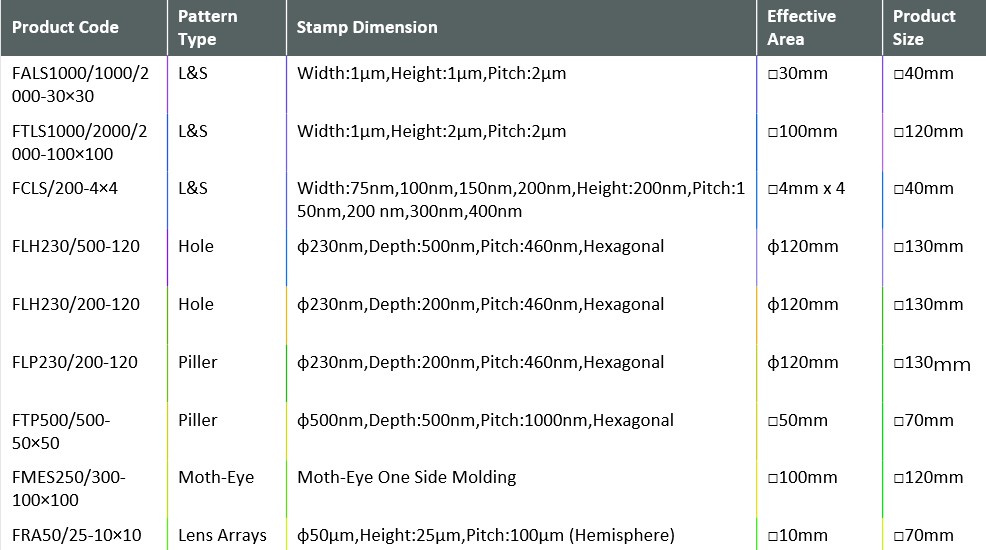
L & S
| Commodity Code | Dimension of Structure | Effective Area | Stamp Dimension | Material | Array |
|
MRLS50/130/100-10×10 |
Width:50nm, Height:130nm, Pitch:100nm |
□10mm |
□10mm |
Silicon(Si) |
–
|
|
MRLS50/130/100-30×30 |
Width:50nm, Height:130nm, Pitch:100nm |
□30mm |
□30mm |
Silicon(Si) |
– |
|
MRLS50/130/100-100×100 |
Width:50nm, Height:130nm, Pitch:100nm |
□100mm |
□100mm |
Silicon(Si) |
– |
|
MTPL50/130/100-300 |
Width:50nm, Height:130nm, Pitch:100nm |
φ280㎜ |
φ300㎜ |
Silicon(Si) |
– |
|
MRLS70/150/140-10×10 |
Width:70nm, Height:150nm, Pitch:140nm |
□10mm |
□10mm |
Silicon(Si) |
– |
|
MRLS70/150/140-300 |
Width:70nm, Height:150nm, Pitch:140nm |
φ280㎜ |
φ3Width:1μm, Height:1μm, Pitch:2μm 00㎜ |
Silicon(Si) |
– |
|
MTLS1/1/2-30×30 |
Width:70nm, Height:150nm, Pitch:140nm |
□30mm |
□30mm |
Silicon(Si) |
– |
Hole
| Commodity Code | Dimension of Structure | Effective Area | Stamp Dimension | Material | Array |
|
MLH230/200/460-30×30 |
φ230nm, Depth:200nm, Pitch:460nm |
□30mm |
□30mm |
Silicon(Si) |
Hexagonal |
|
MLH230/200/460-50×50 |
φ230nm, Depth:200nm, Pitch:460nm |
□50mm |
□50mm |
Silicon(Si) |
Hexagonal |
|
MLH230/200/460-φ120 |
φ230nm, Depth:200nm, Pitch:460nm |
φ120mm |
φ120mm |
Silicon(Si) |
Hexagonal |
|
MTH500/500/1000-30×30 |
φ500nm, Depth:500nm, Pitch:1000nm |
□30mm |
□30mm |
Silicon(Si) |
Hexagonal |
|
MTH500/500/1000-50×50 |
φ500nm, Depth:500nm, Pitch:1000nm |
□50mm |
□50mm |
Silicon(Si) |
Hexagonal |
Pillar
| Commodity Code | Dimension of Structure | Effective Area | Stamp Dimension | Material | Array |
|
MLP230/500/460-30×30 |
φ230nm, Height:500nm, Pitch:460nm |
□30mm |
□30mm |
Silicon(Si) |
Hexagonal |
|
MLP230/500/460-φ120 |
φ230nm, Height:500nm, Pitch:460nm |
φ120mm |
φ120mm |
Silicon(Si) |
Hexagonal |
|
MLP230/200/460-30×30 |
φ230nm, Height:200nm, Pitch:460nm |
□30mm |
□30mm |
Silicon(Si) |
Hexagonal |
|
MLP230/200/460-φ120 |
φ230nm, Height:200nm, Pitch:460nm |
φ120mm |
φ120mm |
Silicon(Si) |
Hexagonal |
|
NAP230/240-100 |
φ230nm, Height:240nm, Pitch:460nm |
□100mm |
□100mm |
Silicon(Si) |
Hexagonal |
Product Contact
Sammi Hsieh
- TOPCO SCIENTIFIC CO.,LTD.
- Senior Manager
- Sales Dept. II, Application Products Div., 1st Business Unit